FPGAs for Software Engineers
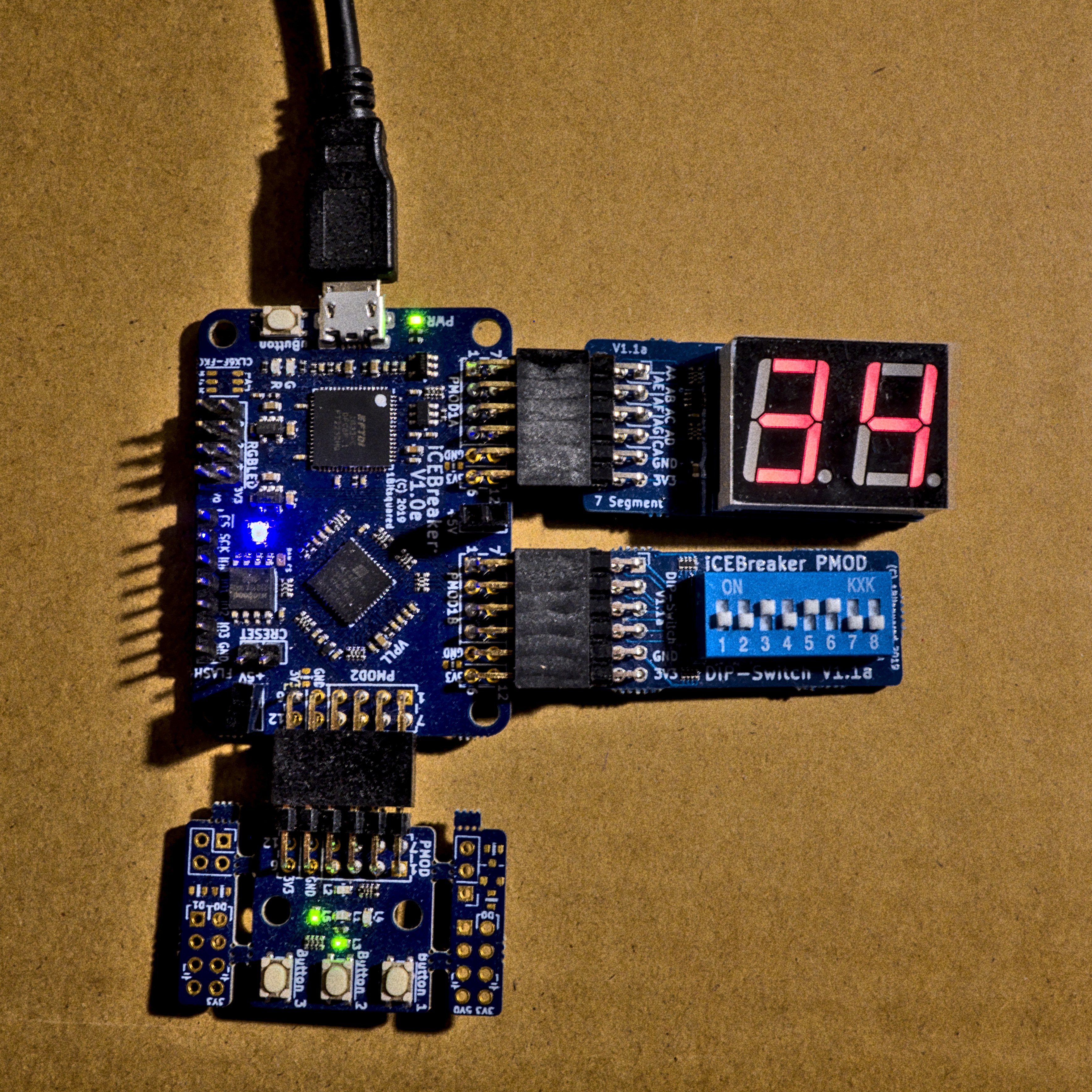
This is an intro into FPGA programming for Software Engineers. It uses the iCEBreaker development board and focuses on Open Source.
OSS Toolchain
If you buy the WTFpga started kit, you can use their provided code and tutorial to get started. It uses Project IceStorm, which itself requires multiple tools. This seems complicated, but even your C/C++/Rust/… compiler uses multiple steps under the hood. The “compilation” steps are:
- Yosys: Verilog synthesis.
- nextpnr: Place and route.
- IceStorm Tools: Required for bitstream generation as well as programming the FPGA chip.
You can either get them from your Linux distribution or if you prefer a rather fresh build (these tools are under very active development), either build them yourself or get nightly binary builds from FPGA-Toolchain. I will explain what all these parts do in detail in the following subsections.
Synthesis
The first step is the “synthesis”, which is basically the following: “How do the declarations in my source code map to the hardware parts available in my FPGA, just looking at the parts.” So it will take your Verilog/VHDL/… code and maps it to LUTs, ALUs, DSPs, and other hardware elements. This is somewhat similar to compiling C/C++/Rust/… to machine code without linking it.
Assuming you have some Verilog code (only one of the files is shown here, you can find the others in the WTFpga repo):
`timescale 1ns / 1ps

module seven_seg_mux(
    input clk,
    input [6:0] disp0, disp1,
    output reg [6:0] segout,
    output disp_sel
);

    reg current;

    assign disp_sel = current;

    always @(posedge clk)
    case (current)
        1:begin
            segout <= disp1;
            current <= 0;
        end
        0:begin
            segout <= disp0;
            current <= 1;
        end
    endcase
endmodule
First, we can use Yosys to plot our files:
yosys -ql wtfpga.log \
    -p 'show -format svg -prefix wtfpga.v' \
    wtfpga.v
Then we can synthesize all our files into a single design:
yosys -ql wtfpga.log \
    -p 'synth_ice40 -top top -json wtfpga.json' \
    wtfpga.v clkdiv.v seven_seg_hex.v seven_seg_mux.v
Yosys will print a bunch of helpful information:
5.50. Printing statistics.

=== top ===

   Number of wires:                 84
   Number of wire bits:            218
   Number of public wires:          84
   Number of public wire bits:     218
   Number of memories:               0
   Number of memory bits:            0
   Number of processes:              0
   Number of cells:                138
     SB_CARRY                       28
     SB_DFF                         24
     SB_DFFN                         8
     SB_LUT4                        78
The machine-readable output is a >16k lines long JSON that describes the parts of the design without actually setting the physical layout. For that, we need the next step.
To get a better idea what was generated we can again generate a graphical output:
yosys -ql wtfpga.log \
    -p 'synth_ice40 -top top -json wtfpga.json' \
    -p 'show -format svg -prefix final' \
    wtfpga.v clkdiv.v seven_seg_hex.v seven_seg_mux.v
Note that yosys can be controlled by some simple embedded programming language (the sections behind the -p parameters) and that synth_ice40 consists of multiple steps.
Place And Route
Now that we have a list of elements that we want to put into our FPGA, the next processing step would be to actually fit them into the physical layout. For machine code coming from your ordinary compiler, this step is kinda easy (given that you work with Random Access Memory and ignore projects like BOLT and LLVM Propeller). For FPGAs it is a bit more tricky. See, there are actual physical parts and wires and latencies between all these components and finding a space (“place”) and a good connection (“route”) given the limited hardware resources (you just have a limited number of wires) is far from trivial (actually it can be NP-hard). Also note that this step can actually make a very large difference in the final result, e.g. if your design can fulfill timing requirements for external connections like displays, USB ports, memory components etc. So this step can, depending on the size of the design, require substantial time and computation resources.
Here is how you do it:
nextpnr-ice40 \
    --up5k \
    --json wtfpga.json \
    --pcf icebreaker.pcf \
    --asc wtfpga.asc
Nextpnr will provide you with a solid amount of information as well:
Info: Critical path report for cross-domain path 'negedge BTN_N$SB_IO_IN_$glb_clk' -> 'posedge displayClock_$glb_clk':
Info: curr total
Info:  1.4  1.4  Source storedValue_SB_DFFN_Q_7_DFFLC.O
Info:  1.8  3.2    Net storedValue[0] budget 4.347000 ns (4,3) -> (5,2)
Info:                Sink div_SB_LUT4_O_7_I2_SB_LUT4_O_LC.I3
...
Info:  2.3 19.6    Net display.segout_SB_DFF_Q_5_D_SB_LUT4_O_I2 budget 5.638000 ns (5,1) -> (7,1)
Info:                Sink display.segout_SB_DFF_Q_5_D_SB_LUT4_O_LC.I2
Info:  1.2 20.8  Setup display.segout_SB_DFF_Q_5_D_SB_LUT4_O_LC.I2
Info: 9.0 ns logic, 11.7 ns routing

...

Info: Max delay <async>                         -> <async>                        : 8.10 ns
Info: Max delay <async>                         -> negedge BTN_N$SB_IO_IN_$glb_clk: 8.83 ns
Info: Max delay <async>                         -> posedge displayClock_$glb_clk  : 21.98 ns
Info: Max delay negedge BTN_N$SB_IO_IN_$glb_clk -> posedge displayClock_$glb_clk  : 20.75 ns
Info: Max delay posedge displayClock_$glb_clk   -> <async>                        : 4.34 ns
So there you can see the longest paths in our design and potential delays, which gives you an idea how fast the design could run. You may wonder what the .pcf file is. It is a Physical Constraints File and maps human-readable names of our design inputs and outputs to physical pins / inputs / outputs of the FPGA chip. These are usually only specified by numeric indices (kinda like a linker script allows you to map memory region names to addresses):
# 12 MHz clock
set_io -nowarn CLK        35

# RS232
set_io -nowarn RX          6
set_io -nowarn TX          9

# LEDs and Button
set_io -nowarn BTN_N      10
set_io -nowarn LEDR_N     11
set_io -nowarn LEDG_N     37

# RGB LED Driver
set_io -nowarn LED_RED_N  39
set_io -nowarn LED_GRN_N  40
set_io -nowarn LED_BLU_N  41
...
Nextpnr has another feature which will generate a visual representation of your placed-and-routed design:
nextpnr-ice40 \
    --gui \
    --up5k \
    --package sg48 \
    --json wtfpga.json \
    --pcf icebreaker.pcf
Be careful, the output SVG is massive and I had some trouble rendering it. Batik does the job reasonable well:
java -Xmx6g -jar batik-rasterizer-1.12.jar -h 1000 routing.svgSo here how it looks like:
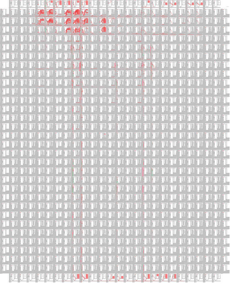
What you see here is some kind of floorplan where the used parts and wires are marked. The WTFpga tutorial is a very small project so there is loads of space left.
Bitcode Generation / Analysis
The last part in our pipeline is the bitcode generation. So here are going to use icestorm:
icepack wtfpga.asc wtfpga.binThen you can flash the binary onto your FPGA:
iceprog wtfpga.binThat’s it. The FPGA now runs the design. BTW: The bitcode format is proprietary and it took the OSS community and some smart people quite some time to reverse-engineer it. So while the toolchain presented here is open source, the official ecosystem and vendor tools and formats are still closed.
Icestorm also offers you some analysis tool to re-check the timings from the place-and-route step:
icetime \
    -d up5k \
    -mtr wtfpga.rpt \
    wtfpga.asc
There you can see that our design runs at least with 40MHz:
icetime topological timing analysis report
==========================================

Info: max_span_hack is enabled: estimate is conservative.

...

Total number of logic levels: 10
Total path delay: 22.99 ns (43.51 MHz)
Build Tools
WTFpga comes with a Makefile-based toolchain. While this is OK to get started, it makes larger projects complex to handle.
One alternative is apio and simplifies the handling of the different tools a lot. It even auto-downloads required tools.
One issue that you might encounter and that seems like a total no-brainer when dialing with “normal software” are dependency managing and building large projects with nested folder structures. For this, have a look at FuseSoC or hdlmake. If you use another language (see languages section), you can use the language-native build tools.
Libraries
If you are wondering if your have to write all your FPGA code yourself or if there is something like npm, PyPi or crates.io and you can just get all the libraries you want in a matter of minutes, I have a good and a bad message for you. The good part is, there are some library (or “core”, which is how they call it) collections:
However, they are far from the convenience that you might expect.
Languages
There are a bunch of languages that you can use to write FPGA code. For example, there is Verilog which is somewhat the C of FPGAs. It has many quirks and from a language-design perspective is somewhat horrible (type-safety anyone?). This might also be due to the fact that it was not really designed to synthesize design but to test them. See this post to get an idea what the differences between “synthesizable” and “not synthesizable” are, and the testing section below for why non sythesizable features might be desried.
Then there is SystemVerilog which kinda feels like the C++ for FPGAs. It is basically a heavily extended Verilog and seems to be used by many.
If you are in Europe, you may also see VHDL quite often. It seems to be the better language compared to Verilog and there is even a Yosys VHDL frontend, however many tools and libraries still use (System)Verilog.
For people who kept an eye on software programming languages, you may have seen that code generation / macros / meta-programming is something that, even though introduced a long time back, has a comeback (just have a look at Rusts procedural macros). The reason is that sometimes it is easier to write code that produces the desired code (e.g. for serialization routines) than it is to find complicated abstractions or template constructs, or to use an external code generator. The same is true for FPGAs, especially because the structures that you put into code are declarative, not impactive. For example, the question to design an integer adder for a given bitwidth can be expressed in terms of code generation in a reusable, and elegant way. You might already know Jinja2 which does something similar for HTML, YAML and others. So you can code FPGA from “normal” programming languages like:
I also have to admit that these languages often provide a way better usability (IDE support, documentation tooling, code formatters, etc.) and allow more modern (or at least for software engineers more familiar) design patterns. So I have ported WTFpga to Chisel and added some CI and simple Makefile-based drivers.
You may wonder how all these languages integrate into the shown software stack. It depends. Some (like nMigen) use Yosys and its intermediate language directly. There are also cross-project intermediate representations like FIRRTL, altough Yosys only seems to be able to produce, not to consume it. And then there is the trick that worked for good old C as well: using an established language — Verilog in this case — as an intermediate target (Chisel can do that). While the latter one enables a wide range of frontend language to thrive and to use compilation, simulation and verification tools, it also has its own challenges when it comes to debugging (variable naming is already a bit of a mess).
Testing
As a good software engineer, you may wonder how testing (and maybe even TDD) works in the world of FPGAs. Now you have been warned, it is a bit more complex than in the software world. When you test software you usually use the software you have just written to test itself. What I mean by that is that you run the software on a CPU, mostly in an environment that is technically somewhat comparable to the target system. Also, the very same CPU that executes your code can be used to reason about it via assertions or even debugging. For FPGAs this seems to be a bit more tricky, since the target environment normally lacks the features to test your design in a reasonable detailed manner. Also, inserting probes into your design might mess up routing and resulting timing, so you may not be able to run the design in the desired frequency anymore. This talk provides an excellent overview over that issue. So what do FPGA designers do? Mostly, there are two paths to follow: simulation and formal verification.
Simulation
Simulation samples the circuit in a sufficient temporal resolution to figure out if given some inputs (including external signals like clocks) the current outputs will follow. The description of the simulation is usually called a “testbench” and you may prefer to write that in the same language as your design.
So you can use Verilog itself with tools like Verilator or Icarus Verilog. I have found the latter semi-convenient since asserts and other assumptions only seem to trigger warning messages which is hard to use for a proper CI test suite. It is however still useful for simulation and debugging. So assuming you have the following testbench to test the display multiplexer of the WTFpga design:
`timescale 1ns / 1ps
module seven_seg_mux_tb;
reg clk = 0;
reg [6:0] disp0 = 13;
reg [6:0] disp1 = 42;
wire [6:0] segout;
wire disp_sel2;
initial
begin
$dumpfile("seven_seg_mux_tb.vcd");
$dumpvars(0, seven_seg_mux_tb);
#10 $finish;
end
always #1 clk = !clk;
seven_seg_mux mux(
.clk(clk),
.disp0(disp0),
.disp1(disp1),
.segout(segout),
.disp_sel(disp_sel2)
);
initial
$monitor(
"At time %t, value = %h (%0d)",
$time, disp_sel2, disp_sel2,
);
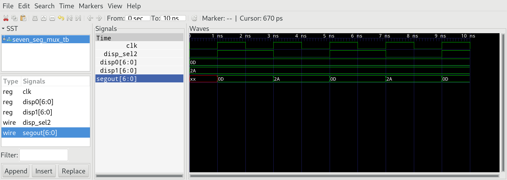
endmoduleYou can use Icarus Verilog to simulate the design:
iverilog \
    -o seven_seg_mux_tb \
    seven_seg_mux_tb.v seven_seg_mux.v

vvp -N seven_seg_mux_tb
This will print some details on the console, but you can also use GTKWave to open the resulting .vcd file:
If you are using Chisel, you can use ChiselTest which uses Treadle by default and works really well for assertions and .vcd outputs.
Another point to integrate simulations would be the primary synthesis toolchain. Yosys offers CXXRTL which can compile design to C++, however this requires you to write some gluecode in C++ and I am not going down that rabbit hole.
Last but not least, if software-based simulations are too slow for your project, you can lift this step to a whole new level using FireSim, which uses FPGAs within the AWS cloud to massively speed up simulations.
Verification
Formal verification is less common amongst software developers, although tools like KLEE and CrossHair exist. Verification always requires some goal you want to proof. This presentation provides a good overview, but here are some things to consider:
- static assertions: Assert that under all valid inputs, the design fulfills some assertions (e.g. the output of a multiplexer equals one of its inputs), time (and especially registers and memory) are not taken into account.
- equivalence: Given two implementations (e.g. a simple but slow baseline and an optimized version), proof that both produce the same outputs under all possible inputs.
- temporal proofs: Similar to static assertions, but over multiple clock steps. These proofs can easily blow up in runtime and memory complexity due to the potential exponentially growing state space (number of static states to the power of clock steps).
awesome-open-hardware-verification provides an overview over possible tools. I am going to focus on SymbiYosys here. There are two files required to proof (at least to a certain extend) that our multiplexer works. First one is the actual proof:
module seven_seg_mux_proof (
    input clk,
    input [6:0] disp0_in, disp1_in,
    output [6:0] segout,
    output disp_sel
);
    reg init = 0;
    reg [6:0] disp0 = 0;
    reg [6:0] disp1 = 0;

    // required for a stable input
    always @(posedge clk) begin
        disp0 <= disp0_in;
        disp1 <= disp1_in;
        init <= 1;
    end

    seven_seg_mux mux(
        .clk(clk),
        .disp0(disp0),
        .disp1(disp1),
        .segout(segout),
        .disp_sel(disp_sel)
    );

`ifdef FORMAL
    always @(posedge clk) begin
        // Need to check both the current and the past value because
        // the same clock signal also drives the mux at the very same
        // moment.
        assert (
            !(init)
            || (segout == disp0)
            || (segout == $past(disp0))
            || (segout == disp1)
            || (segout == $past(disp1))
        );
    end
`endif
endmodule
The second file is an .sby file:
[options]
mode bmc
depth 100

[engines]
smtbmc

[script]
read_verilog seven_seg_mux.v
read_verilog -formal seven_seg_mux_proof.v
prep -top seven_seg_mux_proof

[files]
seven_seg_mux_proof.v
seven_seg_mux.v
Now you can run the proof using the following command:
sby seven_seg_mux.sbyIf the proof fails, it will emit a counterexample as a .vcd file. However be careful with race-conditions, i.e. when using the clock signal both for assertions and as a driver. These conditions are not reflected very well in the resulting waveform.
Other Tools & Further References
If you fancy something more GUI-driven, check out icestudio.
See this slide deck which gives a nice overview over the state-of-the-art of the OSS FPGA landscape. Also check out the wikipedia article about PLLs, which are a fascinating piece of engineering and used in many places.